Difference between revisions of "PCF8591 8-bit A/D and D/A converter Module"
| Line 3: | Line 3: | ||
The PCF8591 module consists of a master control chip PCF8591, some resistors and capacitors .It can data acquisition device and has four analog inputs, one analog output and a serial I2C-bus interface. Three address pins A0, A1 and A2 are used for programming the hardware address, allowing the use of up to eight devices connected to the I2C-bus without additional hardware. Address, control and data to and from the device are transferred serially via the two-line bidirectional I2C-bus. | The PCF8591 module consists of a master control chip PCF8591, some resistors and capacitors .It can data acquisition device and has four analog inputs, one analog output and a serial I2C-bus interface. Three address pins A0, A1 and A2 are used for programming the hardware address, allowing the use of up to eight devices connected to the I2C-bus without additional hardware. Address, control and data to and from the device are transferred serially via the two-line bidirectional I2C-bus. | ||
The schematic diagram of the module is as follows: | The schematic diagram of the module is as follows: | ||
| − | [[File:Cfdf.png]] | + | [[File:Cfdf.png]]<br> |
<font color="red"> | <font color="red"> | ||
Note:<br> | Note:<br> | ||
| Line 27: | Line 27: | ||
*Address by 3 hardware address pins | *Address by 3 hardware address pins | ||
=='''Resource'''== | =='''Resource'''== | ||
| − | [http://www.lengeek.com/wiki/index.php?title=File:PCF8591.PDF PCF8591 datasheet][[File:PDF. | + | [http://www.lengeek.com/wiki/index.php?title=File:PCF8591.PDF PCF8591 datasheet][[File:PDF.jpg]] |
Revision as of 06:49, 24 March 2016
Introduction
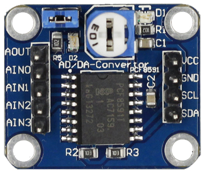
The PCF8591 module consists of a master control chip PCF8591, some resistors and capacitors .It can data acquisition device and has four analog inputs, one analog output and a serial I2C-bus interface. Three address pins A0, A1 and A2 are used for programming the hardware address, allowing the use of up to eight devices connected to the I2C-bus without additional hardware. Address, control and data to and from the device are transferred serially via the two-line bidirectional I2C-bus.
The schematic diagram of the module is as follows:
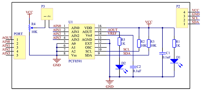
Note:
通过原理图,AIN0上接了一个电位器,如果你用跳线帽接上P3(即电位器旁边的两个引脚),那你就可以用电位器来作为AIN0的输入
By schematics on AIN0 received a potentiometer , if you use the jumper connected to P3 ( ie two pins potentiometer next to it) , then you can potentiometer input as AIN0
PCF8591
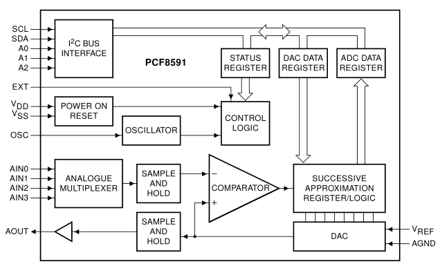
The PCF8591 is a single-chip, single-supply low power 8-bit CMOS data acquisition device with four analog inputs, one analog output and a serial I2C-bus interface. Three address pins A0, A1 and A2 are used for programming the hardware address, allowing the use of up to eight devices connected to the I2C-bus without additional hardware. Address, control and data to and from the device are transferred serially via the two-line bidirectional I2C-bus. The functions of the device include analog input multiplexing, on-chip track and hold function, 8-bit analog-to-digital conversion and an 8-bit digital-to-analog conversion. The maximum conversion rate is given by the maximum speed of the I2C-bus.
Block Diagram
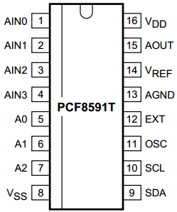
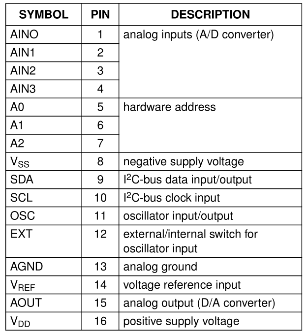
Pin Function
Features
- Support acquisition of external 4-line voltage inputs (ranging 0-5v), with a single power supply
- Standard double-sided printed circuit board, 1.16mm thick, with an elegant layout, 3-mm holes at each corner for easy fixing
- Use an 8-bit successive approximation A/D converter
- Input/output by an I2C bus
- Working voltage: 2.5-6V DC; PCB size: 2.4 x 2.8 cm
- Single supply, low standby current
- Address by 3 hardware address pins
