Difference between revisions of "L293D Motor Driver Shield"
(→L293D) |
|||
| (9 intermediate revisions by the same user not shown) | |||
| Line 1: | Line 1: | ||
='''Introduction'''= | ='''Introduction'''= | ||
[[File:71v-3jELGrL. SL1000 .jpg]]<br> | [[File:71v-3jELGrL. SL1000 .jpg]]<br> | ||
| − | SunFounder L293D is a monolithic integrated, high voltage, high current, 4-channel driver. Basically this means using this chip you can use DC motors and power supplies of up to | + | SunFounder L293D is a monolithic integrated, high voltage, high current, 4-channel driver. Basically this means using this chip you can use DC motors and power supplies of up to 16 Volts, thats some pretty big motors and the chip can supply a maximum current of 600mA per channel, the L293D chip is also what's known as a type of H-Bridge. The H-Bridge is typically an electrical circuit that enables a voltage to be applied across a load in either direction to an output, e.g. motor. |
The schematic diagram is as follows : | The schematic diagram is as follows : | ||
[[File:L293D schematic.png]]<br> | [[File:L293D schematic.png]]<br> | ||
='''L293D'''= | ='''L293D'''= | ||
| − | + | ||
The L293D is quadruple high-current half-H drivers.It is designed to provide bidirectional drive currents of up to 600-mA at voltages from 4.5 V to 36 V. Both devices are designed to drive inductive loads such as relays, solenoids, dc and bipolar stepping motors, as well as other high-current/high-voltage loads in positive-supply applications. | The L293D is quadruple high-current half-H drivers.It is designed to provide bidirectional drive currents of up to 600-mA at voltages from 4.5 V to 36 V. Both devices are designed to drive inductive loads such as relays, solenoids, dc and bipolar stepping motors, as well as other high-current/high-voltage loads in positive-supply applications. | ||
All inputs are TTL compatible. Each output is a complete totem-pole drive circuit, with a Darlington transistor sink and a pseudo- Darlington source. Drivers are enabled in pairs, with drivers 1 and 2 enabled by 1,2EN and drivers 3 and 4 enabled by 3,4EN. When an enable input is high, the associated drivers are enabled, and their outputs are active and in phase with their inputs. When the enable input is low, those drivers are disabled, and their outputs are off and in the high-impedance state. With the proper data inputs, each pair of drivers forms a full-H (or bridge) reversible drive suitable for solenoid or motor applications.<br> | All inputs are TTL compatible. Each output is a complete totem-pole drive circuit, with a Darlington transistor sink and a pseudo- Darlington source. Drivers are enabled in pairs, with drivers 1 and 2 enabled by 1,2EN and drivers 3 and 4 enabled by 3,4EN. When an enable input is high, the associated drivers are enabled, and their outputs are active and in phase with their inputs. When the enable input is low, those drivers are disabled, and their outputs are off and in the high-impedance state. With the proper data inputs, each pair of drivers forms a full-H (or bridge) reversible drive suitable for solenoid or motor applications.<br> | ||
| Line 83: | Line 83: | ||
</center> | </center> | ||
=='''Features'''== | =='''Features'''== | ||
| − | + | *Wide Supply-Voltage Range: 4.5 V to 36 V<br> | |
| − | + | *Separate Input-Logic Supply <br> | |
| − | + | *Internal ESD Protection <br> | |
| − | + | *Thermal Shutdown <br> | |
| − | + | *High-Noise-Immunity Inputs <br> | |
| − | + | *Output Current 600 mA Per Channel<br> | |
| − | + | *Peak Output Current 1.2 A Per Channel<br> | |
| + | |||
='''74HC595'''= | ='''74HC595'''= | ||
[[File:74hc595pi.jpg]]<br> | [[File:74hc595pi.jpg]]<br> | ||
| Line 138: | Line 139: | ||
|} | |} | ||
=='''Features'''== | =='''Features'''== | ||
| − | + | *8-Bit Serial-In, Parallel-Out Shift<br> | |
| − | + | *Wide Operating Voltage Range of 2 V to 6 V<br> | |
| − | + | *High-Current 3-State Outputs Can Drive Up To 15 LSTTL Loads<br> | |
| − | + | *Low Power Consumption, 80-µA Max ICC<br> | |
| − | + | *Typical tpd = 13 ns<br> | |
| − | + | *Low Input Current of 1<br> | |
| − | + | *Shift Register Has Direct Clear<br> | |
| + | |||
='''Resource'''= | ='''Resource'''= | ||
| − | [http:// | + | [http://wiki.sunfounder.cc/images/a/af/L293D_datasheet.pdf L293D_datasheet] [[File:PDF.jpg]]<br> |
| − | [http:// | + | [http://wiki.sunfounder.cc/images/9/9d/74HC595.pdf 74HC595 datasheet] [[File:PDF.jpg]]<br> |
| − | [http:// | + | [http://wiki.sunfounder.cc/images/a/a2/L293D_Module_test_code.zip L293D_Module_test_code] [[File:ZIP.jpg]] |
Latest revision as of 10:12, 22 January 2018
Contents
Introduction
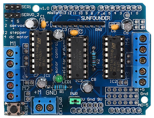
SunFounder L293D is a monolithic integrated, high voltage, high current, 4-channel driver. Basically this means using this chip you can use DC motors and power supplies of up to 16 Volts, thats some pretty big motors and the chip can supply a maximum current of 600mA per channel, the L293D chip is also what's known as a type of H-Bridge. The H-Bridge is typically an electrical circuit that enables a voltage to be applied across a load in either direction to an output, e.g. motor.
The schematic diagram is as follows :
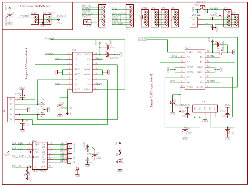
L293D
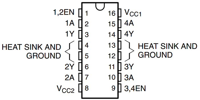
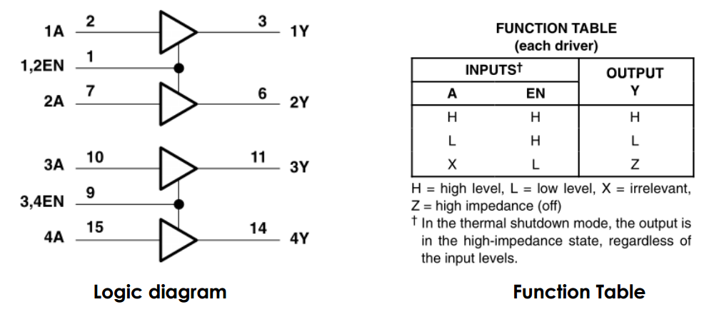
The L293D is quadruple high-current half-H drivers.It is designed to provide bidirectional drive currents of up to 600-mA at voltages from 4.5 V to 36 V. Both devices are designed to drive inductive loads such as relays, solenoids, dc and bipolar stepping motors, as well as other high-current/high-voltage loads in positive-supply applications.
All inputs are TTL compatible. Each output is a complete totem-pole drive circuit, with a Darlington transistor sink and a pseudo- Darlington source. Drivers are enabled in pairs, with drivers 1 and 2 enabled by 1,2EN and drivers 3 and 4 enabled by 3,4EN. When an enable input is high, the associated drivers are enabled, and their outputs are active and in phase with their inputs. When the enable input is low, those drivers are disabled, and their outputs are off and in the high-impedance state. With the proper data inputs, each pair of drivers forms a full-H (or bridge) reversible drive suitable for solenoid or motor applications.
Pin Function
| Pin | Name | Function |
|---|---|---|
| 1 | Enable1,2 | Enable pin to control 1,2 driver |
| 2 | Input 1A | Input to control 1Y |
| 3 | Output 1Y | Output,connect to motor |
| 4 | GND | Ground and heat sink |
| 5 | GND | Ground and heat sink |
| 6 | Output 2Y | Output,connect to motor |
| 7 | Input 2A | Input to control 2Y |
| 8 | Vcc2 | Output supply voltage |
| 9 | Enable3,4 | Enable pin to control 3,4 driver |
| 10 | Input 3A | Input to control 3Y |
| 11 | Output 3Y | Output,connect to motor |
| 12 | GND | Ground and heat sink |
| 13 | GND | Ground and heat sink |
| 14 | Output 4Y | Output,connect to motor |
| 15 | Input 4A | Input to control 4Y |
| 16 | Vcc1 | Supply voltage(7 max) |
Features
- Wide Supply-Voltage Range: 4.5 V to 36 V
- Separate Input-Logic Supply
- Internal ESD Protection
- Thermal Shutdown
- High-Noise-Immunity Inputs
- Output Current 600 mA Per Channel
- Peak Output Current 1.2 A Per Channel
74HC595
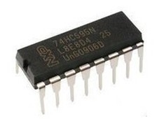
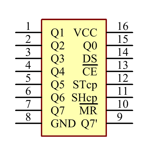
The 74HC595 consists of an 8−bit shift register and a storage register with three−state parallel outputs. It converts serial input into parallel output so that you can save IO ports of an MCU. The 74HC595 is widely used to indicate multipath LEDs and drive multi-bit segment displays. "Three-state" refers to the fact that you can set the output pins as either high, low or "high impedance." With data latching, the instant output will not be affected during the shifting; with data output, you can cascade 74HC595s more easily.
Pin Function
| No | Name | Function |
|---|---|---|
| 1 | Q0-Q7 | 8-bit parallel data output pins, able to control 8 LEDs or 8 pins of 7-segment display directly. |
| 2 | Q7’ | Series output pin, connected to DS of another 74HC595 to connect multiple 74HC595s in series |
| 3 | MR | Reset pin, active at low level; here it is directly connected to 5V. |
| 4 | SHcp | Time sequence input of shift register. On the rising edge, the data in shift register moves successively one biti.e. data in Q1 moves to Q2, and so forth. While on the falling edge, the data in shift register remain unchanged. |
| 5 | STcp | Time sequence input of storage register. On the rising edge, data in the shift register moves into memory register. |
| 6 | OE | Output enable pin, active at low level |
| 7 | DS | Serial data input pin |
| 8 | VCC | Positive supply voltage |
| 9 | GND | Ground |
Features
- 8-Bit Serial-In, Parallel-Out Shift
- Wide Operating Voltage Range of 2 V to 6 V
- High-Current 3-State Outputs Can Drive Up To 15 LSTTL Loads
- Low Power Consumption, 80-µA Max ICC
- Typical tpd = 13 ns
- Low Input Current of 1
- Shift Register Has Direct Clear
