Difference between revisions of "Step-down DC-DC Converter Module"
(→Resource) |
|||
| Line 42: | Line 42: | ||
=='''Features'''== | =='''Features'''== | ||
Fixed output voltage: 5V<br> | Fixed output voltage: 5V<br> | ||
| − | Wide input voltage range, up to | + | Wide input voltage range, up to 12V<br> |
PCB size: 2.5 x 5.0 cm<br> | PCB size: 2.5 x 5.0 cm<br> | ||
Guaranteed 3.0 A Output Load Current <br> | Guaranteed 3.0 A Output Load Current <br> | ||
Latest revision as of 09:49, 4 November 2019
Contents
Introduction
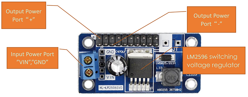
The DC-DC module is used to reduce the input voltage and output stable 5 volts voltage. Here the LM2596 switching voltage regulator is used to regulate the voltage.

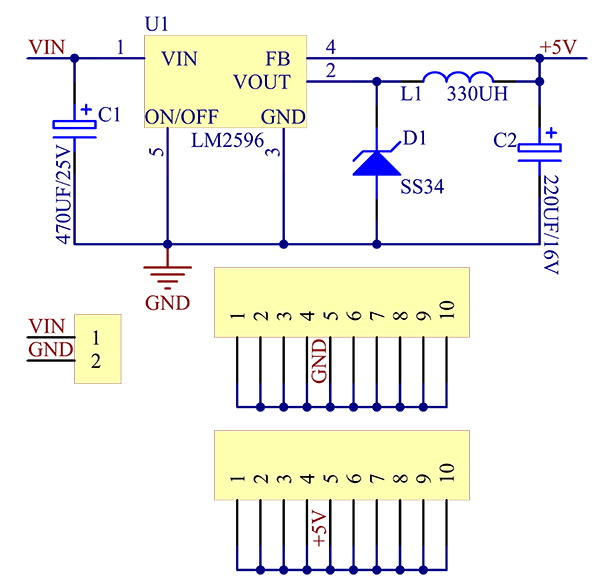
The corresponding schematic diagram is as shown in following:

Introduction of LM2596
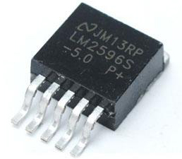
The LM2596 regulator is monolithic integrated circuit ideally suited for easy and convenient design of a step−down switching regulator (buck converter). It is capable of driving a 3.0 A load with excellent line and load regulation. It is internally compensated to minimize the number of external components to simplify the power supply design.
Since LM2596 converter is a switch−mode power supply, its efficiency is significantly higher in comparison with popular three−terminal linear regulators, especially with higher input voltages. The LM2596 operates at a switching frequency of 150 kHz thus allowing smaller sized filter components than what would be needed with lower frequency switching regulators. Available in a standard 5−lead TO−220 package with several different lead bend options, and D2PAK surface mount package.
The other features include a guaranteed 4% tolerance on output voltage within specified input voltages and output load conditions, and 15% on the oscillator frequency. External shutdown is included, featuring 80 A (typical) standby current. Self-protection features include switch cycle−by−cycle current limit for the output switch, as well as thermal shutdown for complete protection under fault conditions.
Pin diagram and Function
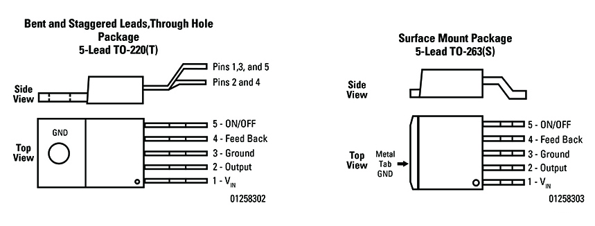
 Its pin functions are as shown in following:
| Pin | Name | Description |
|---|---|---|
| 1 | VIN | This is the positive input supply for the IC switching regulator. A suitable input by pass capacitor must be present at this pin to minimize voltage transients and to supply the switching currents needed by the regulator. |
| 2 | GND | Circuit ground |
| 3 | OUTPUT | Internal switch. The voltage at this pin switches between (+V IN − V SAT) and approximately −0.5V, with a duty cycle of approximately V OUT /V IN. To minimize coupling to sensitive circuitry, the PC board copper area connected to this pin should be kept to a minimum |
| 4 | Feedback | Senses the regulated output voltage to complete the feedback loop |
| 5 | ON/OFF | Allows the switching regulator circuit to be shut down using logic level signals thus dropping the total input supply current to approximately 80 µA. Pulling this pin below a threshold voltage of approximately 1.3V turns the regulator on, and pulling this pin above 1.3V (up to a maximum of 25V) shuts the regulator down. If this shutdown feature is not needed, the ON /OFF pin can be wired to the ground pin or it can be left open; in either case the regulator will be in the ON condition |
Features
Fixed output voltage: 5V
Wide input voltage range, up to 12V
PCB size: 2.5 x 5.0 cm
Guaranteed 3.0 A Output Load Current
150 kHz Fixed Frequency Internal Oscillator
TTL Shutdown Capability
Low Power Standby Mode, typ 80 μA
Thermal Shutdown and Current Limit Protection
Internal Loop Compensation
Moisture Sensitivity Level (MSL) Equals 1
High efficiency
Applications
Simple high-efficiency step-down (buck) regulator
On-card switching regulators
Positive to negative converter

